
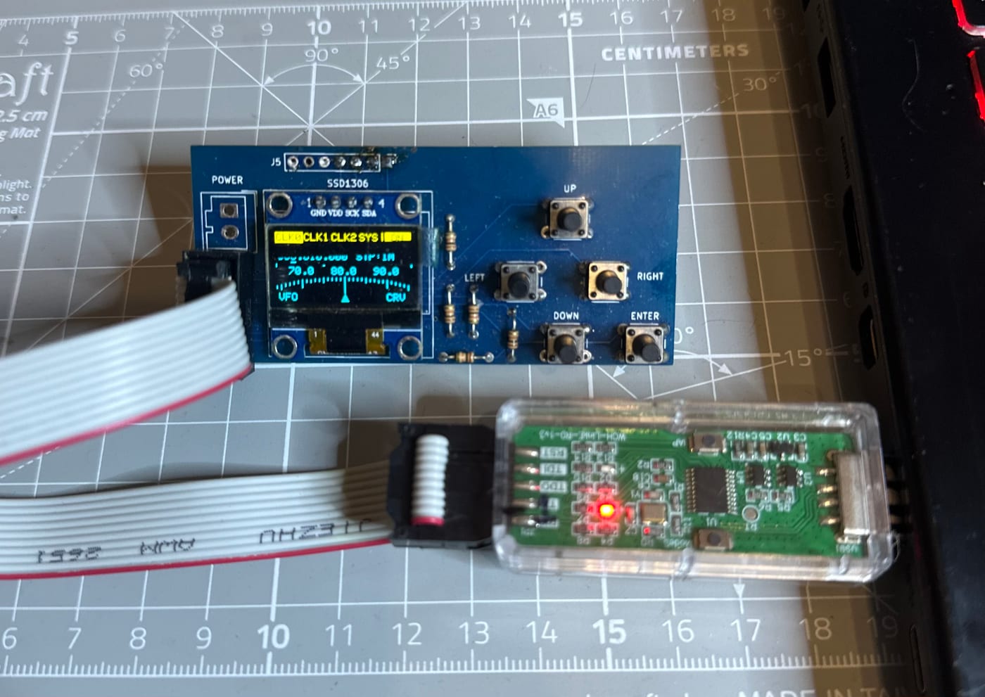
Embeetle IDE + WCH CH32V003 + Si5351A + SSD1306 OLED Signal Generator Tutorial







Source Code & KiCad PCB:
- Firmware & Embeetle Project: roboter/Hardware/WCH/ch32v003f4p6-SignalGenerator
- KiCad Schematic & PCB (v1): roboter/Hardware/WCH/KiCAD/SignalGenerator (v1)
Interactive Companion Tool: Use the Si5351A Interactive Configurator & Register Workbench to visualize PLL/MultiSynth routing, verify register bitfields, and export ready-to-compile CH32V003 Bare-Metal C headers straight into your Embeetle project.
In this tutorial, you will learn how to build a complete, bare-metal 3-channel RF Signal Generator & Retro Vernier VFO (10 kHz – 200 MHz per datasheet, overclockable up to 225 MHz) using an ultra-low-cost WCH CH32V003F4P6 RISC-V microcontroller (only 16 KB Flash and 2 KB SRAM), a Silicon Labs Si5351A clock generator, a 128×64 dual-color SSD1306 OLED display, and Embeetle IDE with a WCH-LinkE programmer.
Table of Contents
- 1. Project Overview & Architecture
- 2. Bill of Materials (BOM)
- 3. Hardware Wiring & Pinout
- 4. PCB & KiCad Project
- 5. Setting Up Embeetle IDE for WCH CH32V003
- 6. Building & Flashing (Embeetle GUI + Optional PowerShell CLI)
- 7. Firmware Deep Dive
- 7.1 Shared 400 kHz Hardware I²C1 Initialization
- 7.2 Driving the Si5351A Clock Generator
- 7.3 Exporting Custom Presets from the Si5351A Workbench
- 7.4 How SSD1306 Display Drawing Works (Pages, Framebuffer & I²C Flush)
- 7.5 How the Limit Gauge & Parabolic Drum Dial Are Drawn
- 7.6 Button State Machine (Focus Modes, Long-Press, Auto-Repeat)
- 8. Operating the Signal Generator
- 9. Troubleshooting & CH32V003 Tips
1. Project Overview & Architecture
The entire system runs on a single $0.15 WCH CH32V003F4P6 (48 MHz RV32EC core) while sharing one hardware I2C1 bus (400 kHz Fast Mode) between the SSD1306 OLED (0x3C) and the Si5351A (0x60):
| Subsystem | Device / Peripheral | Address / Pins | Role |
|---|---|---|---|
| MCU | WCH CH32V003F4P6 | 48 MHz, 16 KB Flash, 2 KB RAM | UI rendering, button polling, I²C master |
| Debugger | WCH-LinkE (R0-1v3) |
PD1 (SWIO), 3V3, GND |
Flashing & debugging via OpenOCD (wlinke) |
| RF Synth | Si5351A (CJMCU-5351, 25 MHz XTAL) | I²C1 0x60 (PC1/PC2) |
3 outputs (CLK0–CLK2), 10 kHz – 200 MHz (up to 225 MHz OC) |
| Display | 0.96” SSD1306 128×64 OLED | I²C1 0x3C (PC1/PC2) |
16 px yellow tab bar + 48 px blue drum dial |
| Controls | 5 Tactile Switches | PC3–PC7 (GPIOC, active-high) |
ENTER, DOWN, LEFT, RIGHT, UP |
Frequency Range Note (Datasheet
200 MHzvs.225 MHzOverclock): According to the official Silicon Labs Si5351A datasheet, the manufacturer-guaranteed output range is2.5 kHz / 8 kHz – 200 MHz(with the internal PLL VCO inside600 – 900 MHz). The firmware allows tuning up to225 MHzby overclocking the PLL slightly above900 MHz—an undocumented mode that works reliably on mostCJMCU-5351boards in practice, though it is not guaranteed across all chips or temperatures.
Key Firmware Features
- 3 Independent Channels (
CLK0,CLK1,CLK2) with individual frequencies, tuning steps (1 Hzto100 MHz), andON/OFFstates. - Zero-Extra-RAM Retro Vernier Drum Dial: Computed column-by-column using integer parabolic droop (
dx² >> 9) and written straight into the existing1,024-byteSSD1306 framebuffer—requiring zero extra RAM buffers and zero floating-point math. - IF Offset Support: Switch between
VFO(0 Hz),+455 kHz(AM/SW IF), and+10.7 MHz(FM/VHF IF) local oscillator modes. - Tight Memory Footprint (
-Og): 16,380 / 16,384 bytes Flash and 1,496 / 2,048 bytes SRAM (including the 1,024-byte OLED framebuffer and 256-byte stack).
2. Bill of Materials (BOM)
| Component | Qty | Notes |
|---|---|---|
| WCH CH32V003F4P6 | 1 | TSSOP-20 breakout board or custom PCB |
| WCH-LinkE Programmer | 1 | Use the LinkE (blue/transparent) version in RISC-V mode |
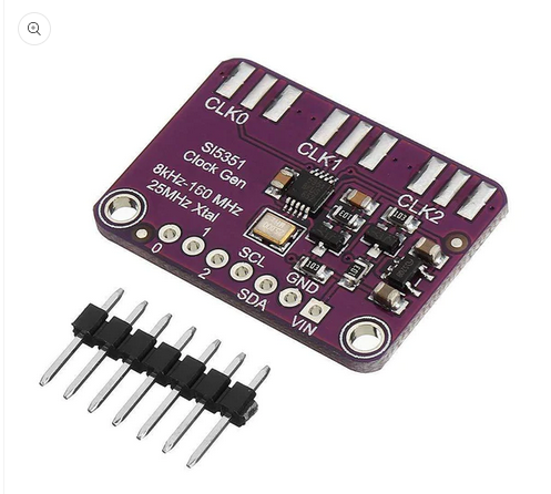
| Si5351A Breakout (CJMCU-5351) | 1 | 25 MHz crystal, 3.3V–5V VIN (with onboard LDO & I²C level shifters) |
| 0.96” SSD1306 I²C OLED (128×64) | 1 | Dual-color (16 px yellow top + 48 px blue bottom) works best |
| Tactile Push Buttons | 5 | UP, DOWN, LEFT, RIGHT, ENTER |
| 4.7 kΩ Resistors | 2 | I²C SDA & SCL pull-ups to 3.3V (if not on breakouts) |
| 10 kΩ (or 1 kΩ) Resistors | 5 (optional) | Pull-down resistors from PC3–PC7 to GND for GPIO_Mode_IN_FLOATING (can be omitted if you enable internal pull-downs with GPIO_Mode_IPD) |
| 100 nF Ceramic Capacitors | 3–8 | DC-blocking on CLK0–CLK2 (+ optional hardware debounce on buttons) |
3. Hardware Wiring & Pinout
All peripherals and buttons are routed to Port C (GPIOC), keeping wiring super clean on both breadboards and compact PCBs.
3.1 WCH-LinkE Programming (SWIO)
The CH32V003 uses WCH’s single-wire debug interface (SWIO) on pin PD1:
| WCH-LinkE Pin | CH32V003F4P6 Pin | Purpose |
|---|---|---|
3V3 |
VDD |
Regulated 3.3V supply |
GND |
VSS |
Common ground |
SWDIO |
PD1 (SWIO) |
Single-wire flash & debug |
Important: Do not repurpose
PD1as a standard GPIO unless you have a recovery sequence—locking outSWIOprevents OpenOCD from connecting until the chip is power-cycled with a reset/erase utility.
3.2 Shared I²C Bus: SSD1306 + Si5351A
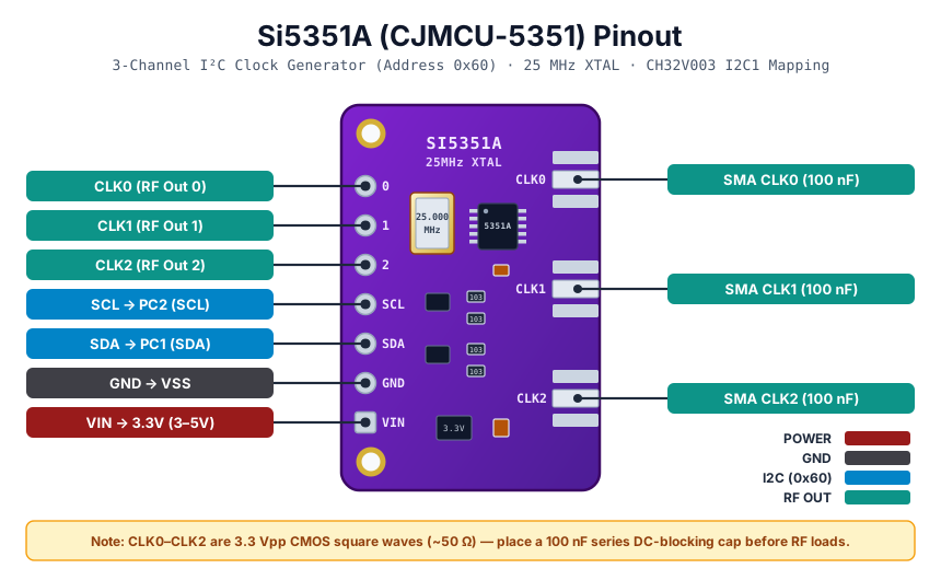
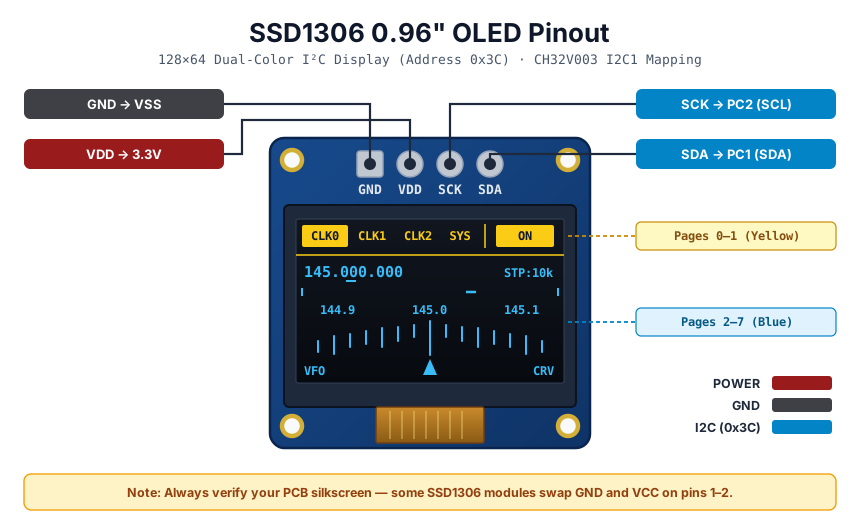
Both the SSD1306 OLED (0x3C) and Si5351A (0x60) share the CH32V003 hardware I2C1 peripheral (AFIO->PCFR1 default mapping 0x00000000) at 400 kHz:
| CH32V003 Pin | Signal | SSD1306 OLED (0x3C) |
Si5351A (0x60) |
|---|---|---|---|
PC1 |
I2C1_SDA |
SDA |
SDA |
PC2 |
I2C1_SCL |
SCL |
SCL |
3.3V |
Power | VDD / VCC |
VIN / VCC |
GND |
Ground | GND |
GND |
Ensure 4.7 kΩ pull-up resistors exist between PC1/PC2 and 3.3V (most CJMCU-5351 and SSD1306 modules include onboard 4.7 kΩ–10 kΩ pull-ups; if both modules have pull-ups in parallel, ~2.2–5 kΩ combined is ideal for 400 kHz Fast Mode).
3.3 5-Way Navigation Buttons
In the stock firmware (source/User/main.h / GPIO_Buttons_INIT()), the 5 navigation buttons are configured as GPIO_Mode_IN_FLOATING (active-high when pressed) to match the external pull-down resistors (R1–R5) on the custom PCB:
| CH32V003 Pin | Macro | Action | Wiring |
|---|---|---|---|
PC3 |
ENTER |
Cycle Focus / Long-press Mute | Switch between 3.3V and PC3 + pull-down to GND |
PC4 |
DOWN |
Decrease Freq / Toggle | Switch between 3.3V and PC4 + pull-down to GND |
PC5 |
LEFT |
Cursor Left / Prev Tab | Switch between 3.3V and PC5 + pull-down to GND |
PC6 |
RIGHT |
Cursor Right / Next Tab | Switch between 3.3V and PC6 + pull-down to GND |
PC7 |
UP |
Increase Freq / Toggle | Switch between 3.3V and PC7 + pull-down to GND |
Simpler Breadboard Tip (No External Pull-Down Resistors Needed): If you are building on a breadboard without the PCB, change
GPIO_Mode_IN_FLOATINGtoGPIO_Mode_IPD(internal pull-down, ~30–50 kΩ) insideGPIO_Buttons_INIT()insource/User/main.c. That lets you drop all 5 external pull-down resistors from the BOM completely—just connect each switch directly between3.3VandPC3–PC7.
3.4 Si5351A RF Output Conditioning
CLK0,CLK1, andCLK2output 3.3 Vpp CMOS square waves with roughly50 Ωsource impedance.- Always place a
100 nFseries capacitor on each output to block DC before connecting to an oscilloscope, spectrum analyzer, mixer, or receiver. - Because CMOS outputs are square waves rich in odd harmonics (
3f,5f,7f), add a low-pass filter (e.g. 5th-order Chebyshev LPF) when you need a clean sine wave.
4. PCB & KiCad Project
Instead of keeping the signal generator on a fragile breadboard, the compact v1 hardware design is packaged as an open-source KiCad 7 project dedicated solely to the CH32V003 + SSD1306 + Si5351A signal generator:
KiCad Project Repository (v1): roboter/Hardware/WCH/KiCAD/SignalGenerator (commit
6942b019)
4.1 Board Specifications (Compact v1 Layout)
| Parameter | Specification |
|---|---|
| EDA Tool | KiCad 7 (version 20221018) |
| Board Dimensions | 78.7 × 35.6 mm (3100 × 1400 mil) — slim pocket-sized handheld layout |
| Stackup | 2-Layer FR-4, 1.6 mm standard thickness (F.Cu + B.Cu) |
| Copper Routing | 19 footprints, 191 straight 45° copper segments (121 Top / 70 Bottom), 7 vias, 32 nets |
| Power Supply | +5V input via J4 (Wago 3.50 mm terminal) → onboard AMS1117-3.3 (U2) regulating to +3.3V |
| Debug & I/O | Dedicated 2×5 WCH-LinkE header (J3), SSD1306 4-pin OLED mount (Brd1), 1×7 Si5351A header (J5), and 5 through-hole tactile switches (SW1–SW5) |
4.2 Top & Bottom PCB Renders
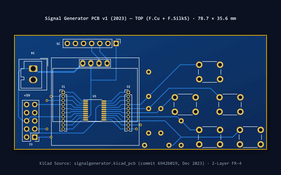
The Top Layer (F.Cu + F.SilkS) places the 0.96” SSD1306 OLED (Brd1) directly above the CH32V003F4P6 MCU (U1) and its dual 1.27 mm pinout headers (J1/J2), with the Si5351A module socket (J5) along the top edge, the +5V Wago terminal (J4) and 10-pin WCH-LinkE header (J3) on the left, and the 5-way through-hole tactile D-pad (SW1–SW5) arranged comfortably for thumb operation on the right:
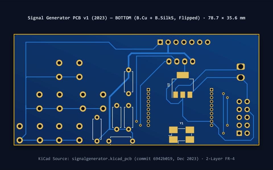
The Bottom Layer (B.Cu + B.SilkS) keeps the front panel clean by tucking the AMS1117-3.3 LDO regulator (U2), the five 1 kΩ axial pull-down resistors (R1–R5), and an optional 24 MHz crystal footprint (Y1) underneath:
4.3 KiCad Project Structure
WCH/KiCAD/SignalGenerator/ (commit 6942b019)
├── SignalGenerator/
│   ├── signalgenerator.kicad_pro     # KiCad 7 project file
│   ├── signalgenerator.kicad_sch     # Full schematic (CH32V003F4P6, SSD1306, Si5351A, AMS1117, switches)
│   ├── signalgenerator.kicad_pcb     # Compact 78.7 × 35.6 mm 2-layer PCB layout (rendered above)
│   └── radme.md                      # Board dimensions (3104 × 1404 mil) & Si5351A design notes
└── WCH-LinkSCH.PDF                   # Reference WCH-Link programmer schematic
4.4 PCB Component & Connector Reference
| Ref | Part / Value | Footprint | Layer | Function |
|---|---|---|---|---|
U1 |
CH32V003F4P6 |
TSSOP-20 (P0.65mm) |
Top | Main 48 MHz RISC-V microcontroller (sits beneath the OLED) |
J1, J2 |
2× 1×10 Pin Header |
1.27 mm vertical |
Top | Full 20-pin breakout of U1 (RX, TX, RST, SWDIO, I2C, buttons) |
Brd1 |
SSD1306 128×64 OLED |
4-pin OLED footprint | Top | GND, +3.3V, SCL, SDA display mount |
J5 |
1×7 Pin Header |
2.54 mm vertical |
Top | Plug-in socket for CJMCU-5351 (Si5351A) (+3.3V, GND, SDA, SCL, CLK0–2) |
J3 |
2×5 Pin Header |
2.54 mm vertical |
Top | Standard 10-pin WCH-LinkE probe header (SWDIO, SWCLK, TX, RX, RST, 3V3, 5V, GND) |
J4 |
Wago 734-132 (1×2) |
3.50 mm terminal |
Top | External +5V / GND power input |
SW1–SW5 |
UP, DOWN, LEFT, RIGHT, ENTER |
6×6 mm THT push-buttons |
Top | 5-way navigation pad on the right side (wired active-high to +3.3V) |
U2 |
AMS1117-3.3 |
SOT-223-3 |
Bottom | +5V → +3.3V LDO voltage regulator |
R1–R5 |
1 kΩ (or 10 kΩ) |
Axial THT (P7.62mm) |
Bottom | Pull-down resistors from SW1–SW5 (PC3–PC7) to GND |
Y1 |
24 MHz Crystal (optional) |
SMD 6.0×3.5 mm 4-pin |
Bottom | Optional external HSE crystal pad (left unpopulated when using internal 48 MHz HSI+PLL) |
4.5 Opening in KiCad & Generating Gerbers
- To inspect or edit in KiCad 7 / 8:
- Download or check out commit
6942b019ofroboter/Hardware. - Open
SignalGenerator/signalgenerator.kicad_proin KiCad. - Open
signalgenerator.kicad_schfor the schematic orsignalgenerator.kicad_pcbto inspect the 2-layer routing and 3D viewer (Alt+3).
- Download or check out commit
- To order the PCB from any fab house (JLCPCB, PCBWay, PCBX, etc.):
- In KiCad PCB Editor, go to File → Fabrication Outputs → Gerbers (
.gbr) (includeF.Cu,B.Cu,F.Mask,B.Mask,F.SilkS,B.SilkS,Edge.Cuts) and click Generate Drill Files (PTH/NPTHExcellon.drl). - Zip the exported
.gbrand.drlfiles and upload using standard 2-layer,1.6 mmFR-4, 1 oz copper settings.
- In KiCad PCB Editor, go to File → Fabrication Outputs → Gerbers (
5. Setting Up Embeetle IDE for WCH CH32V003
Embeetle IDE is a lightweight, makefile-based embedded IDE that ships with preconfigured WCH CH32V003 starter projects, the xPack GNU RISC-V GCC toolchain, and WCH OpenOCD—no complex Eclipse workspaces or proprietary SDK installers required.
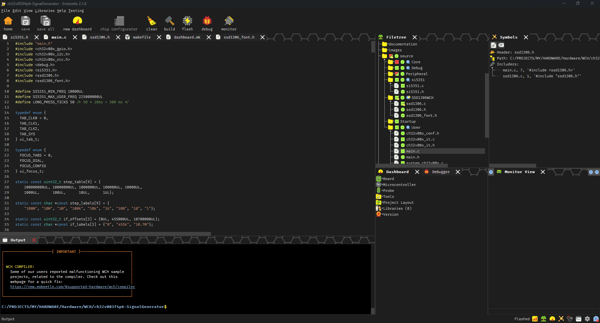
Step 1: Create or Import a CH32V003 Project in Embeetle
- Launch Embeetle IDE and click Create Project (or Open Project if importing an existing repository).
- In the wizard:
- Vendor:
WCH - Board / Chip:
ch32v003f4p6(e.g.ch32v003f4p6-evt-r0-1v1starter) - Probe:
wch-linke-r0-1v3-riscv
- Vendor:
- Embeetle automatically downloads and binds:
gnu_make_4.2.1gnu_riscv_xpack_toolchain(riscv-none-embed-gcc)openocd_wch(openocd.exewith WCH-LinkE support)
5.1 Project Layout & Embeetle Config Files
Organize your project using Embeetle’s clean separation between config/ (build & probe configuration) and source/ (application + drivers):
ch32v003f4p6-SignalGenerator/
├── build/                    # Compiled .o, application.elf, .bin, .hex, output.map
├── config/
│   ├── dashboard.mk          # MCU flags (-march=rv32ec), linker script, paths
│   ├── filetree.mk           # Auto-generated list of checked source files & include dirs
│   ├── linkerscript.ld       # 16 KB Flash / 2 KB SRAM memory map
│   ├── makefile              # Top-level build & flash rules
│   ├── openocd_chip.cfg      # ch32v003f4p6 flash bank & SDI target
│   └── openocd_probe.cfg     # WCH-LinkE adapter driver config
├── source/
│   ├── Core/                 # core_riscv.c / .h
│   ├── Debug/                # Delay_Init, Delay_Ms, USART_Printf_Init
│   ├── Peripheral/           # WCH StdPeriph drivers (gpio, i2c, rcc, usart)
│   ├── Startup/              # startup_ch32v00x.S
│   ├── SSD1306WCH/           # ssd1306.c, ssd1306.h, ssd1306_font.h
│   ├── si5351/               # si5351.c, si5351.h
│   └── User/                 # main.c, main.h, system_ch32v00x.c, ch32v00x_it.c
├── build.ps1                 # Optional PowerShell CLI build script
└── flash.ps1                 # Optional PowerShell CLI flash script
5.2 Using filetree.mk and dashboard.mk (Configured by Default)
Works Right Out of the Box: When you create a
ch32v003f4p6project in Embeetle IDE (or open this repository),dashboard.mk,filetree.mk,openocd_probe.cfg, andopenocd_chip.cfgare already configured by default and should build and flash immediately without manual edits. The snippets below are for reference so you know what Embeetle manages behind the scenes.
One of Embeetle’s best features is its Filetree checkmarks:
- When you drop
source/si5351/andsource/SSD1306WCH/into your project and#include <si5351.h>/#include <ssd1306.h>inmain.c, Embeetle automatically detects them and gives them green checkmarks. - Only checked files are compiled into
config/filetree.mk—so unused WCH peripheral files (like ADC, SPI, TIM) stay excluded and never bloat your 16 KB Flash:
# config/filetree.mk (auto-managed by Embeetle)
C_OFILES = \
  project/source/Debug/debug.c.o \
  project/source/Peripheral/src/ch32v00x_gpio.c.o \
  project/source/Peripheral/src/ch32v00x_i2c.c.o \
  project/source/Peripheral/src/ch32v00x_rcc.c.o \
  project/source/Peripheral/src/ch32v00x_usart.c.o \
  project/source/SSD1306WCH/ssd1306.c.o \
  project/source/User/ch32v00x_it.c.o \
  project/source/User/main.c.o \
  project/source/User/system_ch32v00x.c.o \
  project/source/si5351/si5351.c.o
Meanwhile, config/dashboard.mk comes pre-populated with the exact RISC-V RV32EC compiler flags for CH32V003:
TARGET_COMMONFLAGS = -march=rv32ec \
                     -mabi=ilp32e \
                     -msmall-data-limit=0 \
                     -msave-restore \
                     -fsigned-char \
                     -fno-common
TARGET_LDFLAGS = --specs=nano.specs
Flash-saving tip:
-msave-restoreand--specs=nano.specsare enabled by default and essential on the CH32V003—they replace bulky function prologues/epilogues and standard C libraries with compact stubs.
5.3 WCH-LinkE OpenOCD Configuration & Important Mode Switch Step
Embeetle automatically generates config/openocd_probe.cfg and config/openocd_chip.cfg for wch-linke-r0-1v3-riscv + ch32v003f4p6, so you don’t need to configure OpenOCD manually—it works right away once your probe is in the right mode.
IMPORTANT — Switch Your WCH-LinkE to RISC-V Mode First!
The WCH-LinkE-R0-1v3 supports both ARM and RISC-V protocols, and many units ship in ARM mode (or get toggled accidentally). Before flashing the CH32V003:
- Check the Blue LED when idle (plugged into USB):
- Blue LED OFF = RISC-V Mode (required for CH32V003 — LED blinks only during active flashing/debug)
- Blue LED ON (steady) = ARM Mode (flashing CH32V003 will fail)
- How to switch modes: Press and hold the
ModeSbutton on the WCH-LinkE while plugging it into your PC’s USB port (or switch via WCH-LinkUtility / Embeetle).- Official Embeetle Probe Documentation: See Embeetle WCH-LinkE-R0-1v3 Setup & Mode-Switch Guide for full pinout, driver, and mode-switching instructions.
For reference, the default generated OpenOCD config files are:
# config/openocd_probe.cfg (configured by default)
adapter driver wlinke
adapter speed 6000
transport select sdi
# config/openocd_chip.cfg (configured by default)
wlink_set_address 0x00000000
set _CHIPNAME wch_riscv
sdi newtap $_CHIPNAME cpu -irlen 5 -expected-id 0x00001
set _TARGETNAME $_CHIPNAME.cpu
target create $_TARGETNAME.0 wch_riscv -chain-position $_TARGETNAME
$_TARGETNAME.0 configure -work-area-phys 0x20000000 -work-area-size 10000 -work-area-backup 1
set _FLASHNAME $_CHIPNAME.flash
flash bank $_FLASHNAME wch_riscv 0x00000000 0 0 0 $_TARGETNAME.06. Building & Flashing (Embeetle GUI + Optional PowerShell CLI)
Option A: Inside Embeetle IDE (Recommended — Works Right Away)
- Confirm your WCH-LinkE is in RISC-V mode (blue LED off when idle — see Embeetle WCH-LinkE docs) and connect
3V3,GND, andSWDIO (PD1)to the CH32V003 board. - Click Build (hammer icon) in the top toolbar to compile
build/application.elf,.bin, and.hex. - Click Flash (chip icon) to program the CH32V003 via OpenOCD.
Option B (Optional): Command-Line PowerShell Scripts (build.ps1 & flash.ps1)
Using PowerShell is completely optional—you never need it if you build and flash from Embeetle’s GUI. However, because Embeetle does not have a separate proprietary CLI wrapper and uses standard GNU Make under the hood (with bundled tools in ~/.embeetle/beetle_tools/), these optional scripts let you invoke the exact same make build / make flash commands from VS Code or PowerShell:
# build.ps1
param([switch]$Clean)
$ErrorActionPreference = "Stop"

$MakeExe   = "$env:USERPROFILE/.embeetle/beetle_tools/gnu_make_4.2.1_64b/make.exe"
$ToolPfx   = "$env:USERPROFILE/.embeetle/beetle_tools/gnu_riscv_xpack_toolchain_10.2.0_1.2_64b/bin/riscv-none-embed-"
$FlashTool = "$env:USERPROFILE/.embeetle/beetle_tools/openocd_wch_0.11.0_dev02415_32b/bin/openocd.exe"
$BuildDir  = Join-Path $PSScriptRoot "build"

if ($Clean) {
    & $MakeExe clean -C $BuildDir -f ../config/makefile "TOOLPREFIX=$ToolPfx" "FLASHTOOL=$FlashTool"
}
& $MakeExe build -C $BuildDir -f ../config/makefile "TOOLPREFIX=$ToolPfx" "FLASHTOOL=$FlashTool"
# Build firmware
.\build.ps1
# Clean and rebuild
.\build.ps1 -Clean
# Flash via WCH-LinkE / OpenOCD
.\flash.ps17. Firmware Deep Dive
7.1 Shared 400 kHz Hardware I²C1 Initialization
In source/User/main.c, I2C_HAL_Init() enables I2C1 on PC1 (SDA) and PC2 (SCL) as open-drain alternate functions (GPIO_Mode_AF_OD) and sets the clock divider for 400 kHz Fast Mode (I2C_CKCFGR_FS):
i2c_err_t I2C_HAL_Init(i2c_device_t *dev) {
  RCC_APB1PeriphResetCmd(RCC_APB1Periph_I2C1, ENABLE);
  RCC_APB1PeriphResetCmd(RCC_APB1Periph_I2C1, DISABLE);
  RCC_APB1PeriphClockCmd(RCC_APB1Periph_I2C1, ENABLE);
  RCC_APB2PeriphClockCmd(I2C_PORT_RCC | RCC_APB2Periph_AFIO, ENABLE);

  AFIO->PCFR1 &= ~(0x04400002);
  AFIO->PCFR1 |= I2C_AFIO_REG; /* Default: PC1=SDA, PC2=SCL */

  GPIO_InitTypeDef GPIO_InitStructure = {0};
  GPIO_InitStructure.GPIO_Pin = (1 << I2C_PIN_SDA) | (1 << I2C_PIN_SCL);
  GPIO_InitStructure.GPIO_Mode = GPIO_Mode_AF_OD;
  GPIO_InitStructure.GPIO_Speed = GPIO_Speed_50MHz;
  GPIO_Init(I2C_PORT, &GPIO_InitStructure);

  I2C1->CTLR2 &= ~I2C_CTLR2_FREQ;
  I2C1->CTLR2 |= (SystemCoreClock / 1000000) & I2C_CTLR2_FREQ;

  if (dev->clkr <= 100000) {
    I2C1->CKCFGR = (SystemCoreClock / (2 * dev->clkr)) & I2C_CKCFGR_CCR;
  } else {
    I2C1->CKCFGR =
        ((SystemCoreClock / (3 * dev->clkr)) & I2C_CKCFGR_CCR) | I2C_CKCFGR_FS;
  }

  I2C_Cmd(I2C1, ENABLE);
  return I2C_OK;
}
Both OLED_init() (talking to 0x3C) and SI5351_begin() (talking to 0x60) reuse this single initialized I2C1 peripheral.
7.2 Driving the Si5351A Clock Generator
Notice a classic WCH StdPeriph pitfall: I2C_Send7bitAddress() expects the 7-bit address shifted left by 1 (SI5351_ADDR << 1, i.e., 0x60 << 1 = 0xC0), and every wait loop includes a timeout so a disconnected breakout never hangs the MCU:
i2c_err_t SI5351_write(uint8_t reg, uint8_t data) {
    uint32_t timeout;

    I2C_GenerateSTART(I2C1, ENABLE);
    timeout = I2C_TIMEOUT;
    while (!I2C_CheckEvent(I2C1, I2C_EVENT_MASTER_MODE_SELECT)) {
        if (--timeout == 0) { I2C_GenerateSTOP(I2C1, ENABLE); return I2C_TIMEOUT; }
    }

    I2C_Send7bitAddress(I2C1, SI5351_ADDR << 1, I2C_Direction_Transmitter);
    timeout = I2C_TIMEOUT;
    while (!I2C_CheckEvent(I2C1, I2C_EVENT_MASTER_TRANSMITTER_MODE_SELECTED)) {
        if (I2C_GetFlagStatus(I2C1, I2C_FLAG_AF)) {
            I2C_ClearFlag(I2C1, I2C_FLAG_AF);
            I2C_GenerateSTOP(I2C1, ENABLE);
            return I2C_ERR_NACK;
        }
        if (--timeout == 0) { I2C_GenerateSTOP(I2C1, ENABLE); return I2C_TIMEOUT; }
    }

    I2C_SendData(I2C1, reg);
    timeout = I2C_TIMEOUT;
    while (!I2C_CheckEvent(I2C1, I2C_EVENT_MASTER_BYTE_TRANSMITTING)) {
        if (--timeout == 0) { I2C_GenerateSTOP(I2C1, ENABLE); return I2C_TIMEOUT; }
    }

    I2C_SendData(I2C1, data);
    timeout = I2C_TIMEOUT;
    while (!I2C_CheckEvent(I2C1, I2C_EVENT_MASTER_BYTE_TRANSMITTED)) {
        if (--timeout == 0) { I2C_GenerateSTOP(I2C1, ENABLE); return I2C_TIMEOUT; }
    }

    I2C_GenerateSTOP(I2C1, ENABLE);
    return I2C_OK;
}
When changing frequency or toggling an output, apply_channel_hw() applies the optional IF offset (0, +455 kHz, or +10.7 MHz), updates the channel divider, and updates Register 3 (OEB):
static void apply_channel_hw(uint8_t ch) {
  if (ch >= 3) return;
  uint32_t out_freq = ch_freq[ch] + if_offsets[if_mode];
  if (out_freq > SI5351_MAX_USER_FREQ) out_freq = SI5351_MAX_USER_FREQ;
  SI5351_set_freq(out_freq, (si5351_clock_t)ch, SI5351_PLL_A);
  SI5351_output_enable((si5351_clock_t)ch, ch_enabled[ch] ? true : false);
}
7.3 Exporting Custom Presets from the Si5351A Workbench
Want an exact Quadrature 90° I/Q pair, Differential 180° clock, Spread-Spectrum EMI mode, or AN619 fractional MultiSynth preset without writing floating-point math on the CH32V003?
- Open the Si5351A Interactive Workbench.
- Configure your XTAL load capacitance (
Reg 183), PPM calibration, andCLK0–CLK2frequencies/modes. - Switch to the C Code Export tab and select
CH32V003 (Bare-Metal). - Click
.hto downloadsi5351_config.hintosource/User/. - Provide a one-line wrapper around
SI5351_write()and callsi5351_apply_preset():
#include "si5351.h"
#include "si5351_config.h"

void si5351_i2c_write_reg(uint8_t reg, uint8_t val) {
    SI5351_write(reg, val);
}

/* Inside main() after I2C_HAL_Init(): */
si5351_apply_preset();
7.4 How SSD1306 Display Drawing Works (Pages, Framebuffer & I²C Flush)
Unlike a typical RGB screen where pixels are stored row by row, a monochrome 128×64 SSD1306 OLED organizes its GDDRAM into 8 horizontal pages (Page 0 to Page 7). Each page is 8 pixels tall and 128 columns wide, so every single byte represents a vertical strip of 8 pixels (bit 0 = top pixel, bit 7 = bottom pixel):
Page 0 (Y =  0.. 7)  ┐ 16 px YELLOW ZONE  -> Tab bar [CLK0][CLK1][CLK2][SYS] | ON/OFF
Page 1 (Y =  8..15)  ┘ (dual-color OLED)
──────────────────────────────────────────────────────────────────────────────────────
Page 2 (Y = 16..23)  ┐ 48 px BLUE ZONE    -> Digital frequency readout + STP:10k
Page 3 (Y = 24..31)  │                    -> Active digit caret + Min..Max Limit Gauge (Y=28..30)
Page 4 (Y = 32..39)  │                    -> Sliding major scale numbers (144.9  145.0  145.1)
Page 5 (Y = 40..47)  │                    -> Parabolic Drum Dial (lower 8 bits of 16-bit column)
Page 6 (Y = 48..55)  │                    -> Parabolic Drum Dial (upper 8 bits of 16-bit column)
Page 7 (Y = 56..63)  ┘                    -> VFO/LO label, Center Pointer (▲/△), CRV/FLT
In source/SSD1306WCH/ssd1306.c, the driver keeps a 1,024-byte RAM framebuffer (static uint8_t ssd1306_buffer[128 * 64 / 8]), which takes exactly half of the CH32V003’s 2 KB SRAM. Drawing happens in three flicker-free stages inside layout_ui():
- Clear RAM buffer (
OLED_clear()): Zeroes all 1,024 bytes in SRAM (memset(ssd1306_buffer, 0, 1024)). - Plot pixels, text, and shapes into SRAM (
OLED_drawPixel()): Maps any(x, y)coordinate to its page index(y / 8)and bit mask(1 << (y & 7)):
void OLED_drawPixel(uint8_t x, uint8_t y, SSD1306_COLOR color) {
    if (x >= SSD1306_WIDTH || y >= SSD1306_HEIGHT) return;

    switch (color) {
        case White:   ssd1306_buffer[x + (y / 8) * 128] |=  (1 << (y & 7)); break;
        case Black:   ssd1306_buffer[x + (y / 8) * 128] &= ~(1 << (y & 7)); break;
        case Inverse: ssd1306_buffer[x + (y / 8) * 128] ^=  (1 << (y & 7)); break;
    }
}- Burst-flush to the OLED over I²C (
OLED_display()/OLED_update()): BecauseOLED_init()configures Horizontal Addressing Mode (0x20, 0x00), flushing the entire frame takes just one address window command (0x00control byte) followed by a single 1,024-byte I²C data stream (0x40control byte):
void OLED_update(void) {
    OLED_sendCommand(SSD1306_COLUMNADDR); OLED_sendCommand(0); OLED_sendCommand(127);
    OLED_sendCommand(SSD1306_PAGEADDR);   OLED_sendCommand(0); OLED_sendCommand(7);

    i2c_start_transmission(SSD1306_I2C_ADDR); /* 0x3C << 1 */
    i2c_write_byte(0x40);                     /* Control byte: GDDRAM data stream */
    for (uint16_t i = 0; i < SSD1306_BUFFER_SIZE; i++) {
        i2c_write_byte(ssd1306_buffer[i]);
    }
    i2c_stop_transmission();
}
At 400 kHz I²C Fast Mode, transferring all 1,024 bytes takes roughly 23 ms (~43 FPS max), which is plenty fast for smooth 14–20 Hz dial scrolling while keeping the display 100% tear- and flicker-free.
7.5 How the Limit Gauge & Parabolic Drum Dial Are Drawn
Instead of calling OLED_drawPixel() hundreds of times per frame or storing heavy bitmaps, draw_retro_dial() in source/User/main.c fetches the raw framebuffer pointer via OLED_getBuffer() and writes bitmasks directly into the SSD1306 pages for both gauges:
1. Full-Range Min–Max Limit Gauge Bar (Page 3, Y = 28..30)
Right below the digital frequency readout sits a compact horizontal gauge showing where the tuned frequency lies across the entire 10 kHz – 225 MHz span:
uint8_t *fb = OLED_getBuffer();

/* Full-range min..max limit gauge bar (Y=28..30 in Page 3) */
uint8_t pos_x = (uint8_t)(f / 1800000UL); /* Maps 0..225 MHz -> X = 0..125 */
if (pos_x > 125) pos_x = 125;             /* Prevent Page 3 overrun into Page 4 */
uint8_t *p3 = fb + 3 * 128;               /* Pointer to Page 3 (Y = 24..31) */
p3[0]         |= 0x70; /* 0b01110000: Left end-stop cap at Y = 28, 29, 30 */
p3[127]       |= 0x70; /* 0b01110000: Right end-stop cap at Y = 28, 29, 30 */
p3[pos_x]     |= 0x20; /* 0b00100000: 2-pixel-wide position cursor at Y = 29 */
p3[pos_x + 1] |= 0x20;
Because Page 3 maps bit 0..7 to Y = 24..31, OR-ing 0x70 (bits 4, 5, 6) draws crisp 3-pixel vertical end-stops at X = 0 and X = 127, while 0x20 (bit 5, Y = 29) draws the moving frequency marker—all in a handful of integer instructions with zero floating-point math. Clamping pos_x to 125 guarantees p3[pos_x + 1] always stays strictly inside the 128-byte Page 3 row (never overwriting the right end-stop at p3[127] or spilling into Page 4 if f ever exceeds 226.8 MHz).
2. Zero-Extra-RAM Parabolic Retro Vernier Drum Dial (Pages 5–6, Y = 40..55)
Below the sliding major scale numbers (Y = 31..39, spaced every 40 px = 10 tuning steps), the vernier drum gauge spans 16 vertical pixels across Page 5 and Page 6 and writes directly into the existing 1 KB OLED framebuffer (requiring zero extra RAM buffers). For each of the 128 horizontal columns, render_dial_column() computes a 16-bit vertical tick pattern on the fly:
- Tick Spacing (
4 pxper step,40 pxper major division):tick_pos == min_pos || max_pos→0x03FF(10 px tall hard limit wall)mod40 == 0→0x00FF(8 px tall major tick)mod40 == 20→0x003E(5 px tall half-division tick)(mod40 & 0x03) == 0→0x000E(3 px tall minor vernier tick)x == 64→0xFFFF(full-height fixed center hairline)
- 3D Cylindrical Drum Illusion (
droop = (dx * dx) >> 9):- Distance from center is
dx = |x - 64|(0at center,64at left/right edges). - Shifting
col_bits << drooppushes ticks downward by0 pxat the center and up to64² / 512 = 8 pxat the edges, creating a smooth parabolic drum curve without any lookup table orsin()/cos().
- Distance from center is
/* Zero-extra-RAM column renderer for Retro Drum Dial (Pages 5..6, Y=40..55) */
static uint16_t render_dial_column(uint8_t x, int32_t center_pos,
                                   int32_t min_pos, int32_t max_pos) {
  if (x == 64)
    return 0xFFFF; /* Fixed center hairline */

  uint8_t droop = 0;
  if (dial_curved) {
    uint16_t dx = (x < 64) ? (uint16_t)(64 - x) : (uint16_t)(x - 64);
    droop = (uint8_t)((dx * dx) >> 9); /* Parabolic drum curvature (0..8 px) */
  }

  int32_t tick_pos = center_pos + ((int32_t)x - 64);
  if (tick_pos < min_pos || tick_pos > max_pos)
    return 0x0000;

  uint16_t col_bits = 0x0000;
  int32_t mod40 = ((tick_pos % 40) + 40) % 40;

  if (tick_pos == min_pos || tick_pos == max_pos) {
    col_bits = 0x03FF; /* Limit stop bar (10 px) */
  } else if (mod40 == 0) {
    col_bits = 0x00FF; /* Major tick (8 px) */
  } else if (mod40 == 20) {
    col_bits = 0x003E; /* Half-way tick (5 px) */
  } else if ((mod40 & 0x03) == 0) {
    col_bits = 0x000E; /* Minor vernier tick (3 px) */
  }

  return (uint16_t)(col_bits << droop);
}
Then draw_retro_dial() splits each 16-bit column directly into Page 5 (low byte) and Page 6 (high byte), and draws the center triangle pointer in Page 7 (OLED_fillTriangle = solid ▲ when ON, OLED_drawTriangle = hollow △ when muted):
for (uint8_t col = 0; col < 128; col++) {
  uint16_t bits = render_dial_column(col, center_pos, min_pos, max_pos);
  fb[5 * 128 + col] |= (uint8_t)(bits & 0xFF);        /* Page 5 (Y = 40..47) */
  fb[6 * 128 + col] |= (uint8_t)((bits >> 8) & 0xFF); /* Page 6 (Y = 48..55) */
}

if (ch_enabled[ch]) {
  OLED_fillTriangle(61, 63, 67, 63, 64, 57, White);   /* Solid ▲ = Output ON */
} else {
  OLED_drawTriangle(61, 63, 67, 63, 64, 57, White);   /* Hollow △ = Muted */
}
Tip:
source/SSD1306WCH/ssd1306.halso includes ready-to-useOLED_drawProgressBar(x, y, w, h, percent)andOLED_drawBargraph(x, y, w, h, bars, filled)helpers if you want to add battery, RF power, or S-meter gauges to your own screens. Similarly,format_freq_str()converts frequencies toXXX.XXX.XXXusing integer math instead ofsprintf(), saving >3 KB of Flash.
7.6 Button State Machine (Focus Modes, Long-Press, Auto-Repeat)
The main loop polls GPIOC every 10 ms (Delay_Ms(10)) and handles:
- Short press on
ENTER(detected on release): Cycles UI focus betweenFOCUS_TABS→FOCUS_DIAL→FOCUS_CONFIG. - Long press on
ENTER(≥ 50 ticks = 500 ms): Mutes or unmutes the active channel immediately (toggling the pointer between solid▲and hollow△). - Hold
UPorDOWNin Dial Focus: After250 ms, accelerates into 14–20 Hz auto-repeat for smooth continuous dial scrolling.
8. Operating the Signal Generator
The dual-color SSD1306 splits cleanly into the 16 px yellow header (tabs + ON/OFF badge) and 48 px blue dial area:
+------------------------------------------+
| [CLK0]  CLK1   CLK2   SYS  |    ON       |  <- 16 px YELLOW BAR (Tabs + Output)
+------------------------------------------+
| 145.000.000               STP:10k        |  <- Digital Readout + Step Size
|     ^                                    |  <- Active Digit Cursor
| |         ===                            |  <- Min..Max Limit Bar (10k..225M)
|  144.9      145.0      145.1             |  <- Sliding Scale Numbers
|   .  |  .  |  .  |  .  |  .  |  .  |     |  <- Parabolic Curved Drum Dial
| VFO               ▲                 CRV  |  <- Mode + Pointer (▲ ON / △ OFF)
+------------------------------------------+| Button | Dial Focus (Default) | Tab Focus | Config Focus |
|---|---|---|---|
UP / DOWN |
Tune frequency (hold for auto-repeat) | Toggle channel ON / OFF |
Toggle DIAL: CURVED/FLAT or IF: 0 / 455k / 10.7M |
LEFT / RIGHT |
Move digit cursor (100M ↔ 1 Hz step) |
Switch CLK0 / CLK1 / CLK2 / SYS |
Select DIAL vs IF setting |
ENTER (Short) |
Cycle focus (Tabs → Dial → Config) | Cycle focus | Cycle focus |
ENTER (Hold 500 ms) |
Mute / Unmute active channel (▲ ↔ △) |
Mute / Unmute | Mute / Unmute |
9. Troubleshooting & CH32V003 Tips
- OpenOCD fails to connect to WCH-LinkE (
Error: wlinke):- Make sure the WCH-LinkE is in RISC-V mode (the blue LED stays off when idle; when the blue LED is on, it is in ARM mode). Hold the
ModeSbutton while plugging in USB or follow Embeetle’s official WCH-LinkE-R0-1v3 documentation. - Check that
SWDIOconnects toPD1(notPD0) and the target has3.3Vpower.
- Make sure the WCH-LinkE is in RISC-V mode (the blue LED stays off when idle; when the blue LED is on, it is in ARM mode). Hold the
- OLED displays
"SI5351 Error!"on boot:- Verify
PC1→SDAandPC2→SCLare not swapped, and both breakouts shareGNDand3.3V. - Confirm your Si5351A responds at 7-bit address
0x60(shifted to0xC0in WCHI2C_Send7bitAddress). - Check that
4.7 kΩpull-ups are present onSDAandSCL.
- Verify
- Linker error:
region FLASH overflowed:- Avoid
printf/sprintfwith%ffloats—stick to integer helpers likeformat_freq_str(). - In Embeetle’s
config/dashboard.mk, switch optimization from-Ogto-Osif you add extra fonts or menu pages.
- Avoid
- Buttons trigger randomly when untouched:
- Because the stock
GPIO_Buttons_INIT()usesGPIO_Mode_IN_FLOATING(matchingR1–R5on the custom PCB), external pull-down resistors toGNDare required onPC3–PC7. On a breadboard, switching the pin mode toGPIO_Mode_IPDenables the CH32V003’s internal pull-downs so you can omit all 5 external pull-down resistors.
- Because the stock
- Output stops or loses lock above
200 MHz:- Silicon Labs guarantees Si5351A operation up to
200 MHz; frequencies from200 MHzto225 MHzrely on overclocking the internal PLL above900 MHz. If your specific chip drops out above200–215 MHz, keepSI5351_MAX_USER_FREQclamped to200000000UL.
- Silicon Labs guarantees Si5351A operation up to
Related Tools & References
- Complete Project Source Code (GitHub): roboter/Hardware/tree/main/WCH/ch32v003f4p6-SignalGenerator — Full Embeetle project, firmware, SSD1306/Si5351 drivers, and wiring guides.
- KiCad Schematic & Compact PCB v1 (GitHub): roboter/Hardware/tree/6942b019/WCH/KiCAD/SignalGenerator — Compact
78.7 × 35.6 mm2-layer PCB (signalgenerator.kicad_pcb) and schematic (signalgenerator.kicad_sch). - Si5351A Interactive Configurator & Register Workbench — Configure PLLs, MultiSynth dividers, phase offsets, and export CH32V003 C register headers.
- WCH SSD1306 OLED Display Driver Post — Earlier Embeetle + CH32V003 SSD1306 driver integration notes.
- Embeetle IDE — WCH-LinkE-R0-1v3 Official Probe Documentation & Mode Switch Guide
- Embeetle IDE — WCH CH32V003 Support
- WCH CH32V003 Datasheet & Reference Manual
- Silicon Labs AN619 — Manually Generating an Si5351 Register Map
Comments
Join the conversation powered by GitHub Discussions.